A Brief History of Nanotechnology

A timeline of important milestones and discoveries in the field of nanotechnology, from ancient nano-sized dye particles to current high-performance products.
- Uploaded on | 2 Views
-
 laurence
About A Brief History of Nanotechnology
PowerPoint presentation about 'A Brief History of Nanotechnology'. This presentation describes the topic on A timeline of important milestones and discoveries in the field of nanotechnology, from ancient nano-sized dye particles to current high-performance products.. The key topics included in this slideshow are Nanotechnology, history, milestones, discoveries, ancient, current,. Download this presentation absolutely free.
Presentation Transcript
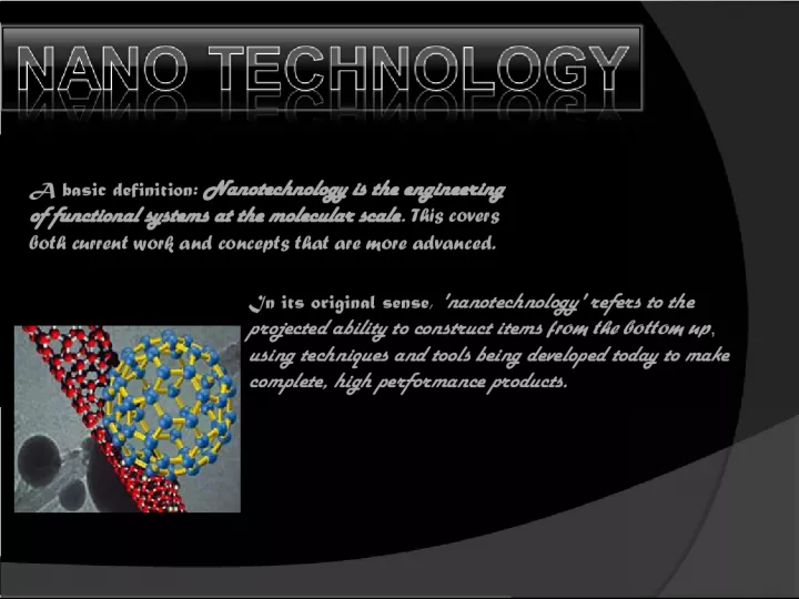
3. A basic definition: Nanotechnology is the engineering of functional systems at the molecular scale . This covers both current work and concepts that are more advanced. In its original sense, 'nanotechnology' refers to the projected ability to construct items from the bottom up , using techniques and tools being developed today to make complete, high performance products.
4. ~ 2000 Years Ago Sulfide nanocrystals used by Greeks and Romans to dye hair ~ 1000 Years Ago (Middle Ages) Gold nanoparticles of different sizes used to produce different colors in stained glass windows 1959 There is plenty of room at the bottom by R. Feynman 1974 Nanotechnology - Taniguchi uses the term nanotechnology for the first time 1981 IBM develops Scanning Tunneling Microscope 1985 Buckyball - Scientists at Rice University and University of Sussex discover C 60 1986 Engines of Creation - First book on nanotechnology by K. Eric Drexler. Atomic Force Microscope invented by Binnig, Quate and Gerbe 1989 IBM logo made with individual atoms 1991 Carbon nanotube discovered by S. Iijima 1999 Nanomedicine 1 st nanomedicine book by R. Freitas 2000 National Nanotechnology Initiative launched
5. K. Eric Drexler (right) popularized the word 'nanotechnology' in the 1980's. he was talking about building machines on the scale of molecules, a few nanometers widemotors, robot arms, and even whole computers, far smaller than a cell. The U.S. National Nanotechnology Initiative was created to fund this kind of nanotech: their definition includes anything smaller than 100 nanometers with novel properties. I want to build a billion tiny factories, models of each other, which are manufacturing simultaneously. . . The principles of physics, as far as I can see, do not speak against the possibility of maneuvering things atom by atom. It is not an attempt to violate any laws; it is something, in principle, that can be done; but in practice, it has not been done because we are too big. Richard Feynman, Nobel Prize winner in physics.
6. Mihail (Mike) Roco of the U.S. National Nanotechnology Initiative has described four generations of nanotechnology development (see chart below):-
7. Carbon nanotubes (CNTs) are allotropes of carbon with a cylindrical nanostructure. Nanotubes have been constructed with length-to-diameter ratio of up to 28,000,000:1,which is significantly larger than any other material. They exhibit extraordinary strength and unique electrical properties, and are efficient thermal conductors . Their final usage, however, may be limited by their potential toxicity. Carbon nanotubes are among the amazing objects that science sometimes creates by accident , without meaning to, but that will likely revolutionize the technological landscape of the century ahead.
8. Carbon nanotubes Carbon nanotubes are fullerene-related structures which consist of graphene cylinders closed at either end with caps containing pentagonal rings . Discovered in 1991 by the Japanese electron microscopist Sumio Iijima . Nanotubes could be produced in bulk quantities by varying the arc-evaporation conditions.
9. The ( n , m ) nanotube naming scheme can be thought of as a vector ( C h ) in an infinite graphene sheet that describes how to "roll up" the graphene sheet to make the nanotube. T denotes the tube axis, and a 1 and a 2 are the unit vectors of graphene in real space. Most single-walled nanotubes (SWNT) have a diameter of close to 1 nanometer, with a tube length that can be many millions of times longer. The structure of a SWNT can be conceptualized by wrapping a one-atom- thick layer of graphite called graphene into a seamless cylinder. The way the graphene sheet is wrapped is represented by a pair of indices ( n , m ) called the chiral vector. The integers n and m denote the number of unit vectors along two directions in the honeycomb crystal lattice of graphene. If m = 0, the nanotubes are called "zigzag". If n = m , the nanotubes are called "armchair". Otherwise, they are called "chiral".
10. Fig. 3.5 (longitudinal view) of a concentric multiwall carbon nanotube (c- MWNT) prepared by electric arc. In insert , sketch of the Russian-doll-like display of graphenes Multi-walled nanotubes (MWNT) consist of multiple rolled layers (concentric tubes) of graphite; In the Russian Doll , sheets of graphite are arranged in concentric cylinders; In the Parchment model, a single sheet of graphite is rolled in around itself, resembling a scroll of parchment or a rolled newspaper. (3.3 );
12. o Smaller, faster, more energy efficient and powerful computing and other IT-based systems More efficient and cost effective technologies for energy production Solar cells Fuel cells Batteries Bio fuels Cancer treatment Bone treatment Drug delivery Appetite control Drug development Medical tools Diagnostic tests Imaging Foods and beverages Advanced packaging materials, sensors, and lab-on- chips for food quality testing Appliances and textiles Stain proof, water proof and wrinkle free textiles Household and cosmetics Self-cleaning and scratch free products, paints, and better cosmetics
13. Nanoscale Materials Nanowires and Nanotubes Lateral dimension: 1 100 nm Nanowires and nanotubes exhibit novel physical, electronic and optical properties due to Two dimensional quantum confinement Structural one dimensionality High surface to volume ratio Potential application in wide range of nanodevices and systems Nanoscale sensors and actuators Photovoltaic devices solar cells Transistors, diodes and LASERs Nanowire Solar Cell: The nanowires create a surface that is able to absorb more sunlight than a flat surface McMaster Univ., 2008
14. Currently available microprocessors use resolutions as small as 32 nm Houses up to a billion transistors in a single chip MEMS based nanochips have future capability of 2 nm cell leading to 1TB memory per chip A NEMS bacteria sensor Nano Lett., 2006, DOI: 10.1021/nl060275y A MEMS based nanochip Nanochip Inc., 2006 NEMS technology enables creation of ultra small and highly sensitive sensors for various applications The NEMS force sensor shown in the figure is applicable in pathogenic bacteria detection Nanoelectromechanical System (NEMS) Sensors
15. Nanoscale materials have feature size less than 100 nm utilized in nano scale structures, devices and systems Nanoparticles and Structures Silver nanoparticles Northwestern Univ., 2002 A stadium shaped quantum corral made by positioning iron atoms on a copper surface IBM Corp., 1993. A 3-dimensional nanostructure grown by controlled nucleation of Silicon-carbide nanowires on Gallium catalyst particles Univ. of Cambridge, 2007 Gold nanoparticles TU Dresden/ESRF, 2008
16. Nanophotonic Systems A silicon processor featuring on-chip nanophotonic network IBM Corp., 2008 Nanophotonic systems work with light signals vs. electrical signals in electronic systems Enable parallel processing that means higher computing capability in a smaller chip Enable realization of optical systems on semiconductor chip Fuel cells use hydrogen and air as fuels and produce water as by product The technology uses a nanomaterial membrane to produce electricity Schematic of a fuel cell Energy solution center Inc. 500 W fuel cell H2economy.com
17. Nanotechnology, Nano structures and engineered nano structures have wide applications in various fields. Many researches are going on featuring the usage of nano in various fields which are resulting in providing great results that one had never imagined of few years ago. If such sort of areas of concern are overridden the field of nanotechnology would lead in creating a world which includes the best goods that one had never imagined when so ever.