Comparison of Gate Current Modeling Approaches for Advanced Gate Stacks and Investigation of Conventional and High-k Insulator Gate Stacks for Sub-50nm MOSFETs

This study aims to investigate the performance and reliability of conventional SiO2 and high-k thin insulator gate stacks for sub-50nm MOSFETs. It includes simulation of C-V and I-V for different gate stack and device architectures, investigation of the effects of high K materials and related defects, traps, charges, and comparison of gate leakage currents in advanced device architectures.
- Uploaded on | 0 Views
-
 cayla
cayla
About Comparison of Gate Current Modeling Approaches for Advanced Gate Stacks and Investigation of Conventional and High-k Insulator Gate Stacks for Sub-50nm MOSFETs
PowerPoint presentation about 'Comparison of Gate Current Modeling Approaches for Advanced Gate Stacks and Investigation of Conventional and High-k Insulator Gate Stacks for Sub-50nm MOSFETs'. This presentation describes the topic on This study aims to investigate the performance and reliability of conventional SiO2 and high-k thin insulator gate stacks for sub-50nm MOSFETs. It includes simulation of C-V and I-V for different gate stack and device architectures, investigation of the effects of high K materials and related defects, traps, charges, and comparison of gate leakage currents in advanced device architectures.. The key topics included in this slideshow are gate current, modeling approaches, gate stacks, sub-50nm MOSFETs, high-k insulator,. Download this presentation absolutely free.
Presentation Transcript
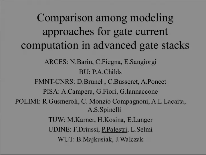
1. Comparison among modeling approaches for gate current computation in advanced gate stacks ARCES: N.Barin, C.Fiegna, E.Sangiorgi BU: P.A.Childs FMNT-CNRS: D.Brunel , C.Busseret, A.Poncet PISA: A.Campera, G.Fiori, G.Iannaccone POLIMI: R.Gusmeroli, C. Monzio Compagnoni, A.L.Lacaita, A.S.Spinelli TUW: M.Karner, H.Kosina, E.Langer UDINE: F.Driussi, P.Palestri , L.Selmi WUT: B.Majkusiak, J.Walczak
2. Aim of Task 3 of SINANO Work-Package 4 Study of the performance and reliability of conventional (SiO2) and high-k thin insulator gate stacks for sub-50nm MOSFETs ) To support the understanding of device reliability issues and potential limitations of device performance related to the gate stack architecture of future CMOS technologies. The activities foreseen in this context are: simulation of C/V and I/V for different gate stack and device architectures; investigation of the effects of high-K materials and of the related defects, traps, charges, etc.. on the low-field mobility and carrier transport properties of the inversion channel. Two main phases : comparison of gate leakage currents in advanced device architectures; assessment of modeling requirements for ultra-thin oxide and high-k, metal gate stacks.
3. OUTLINE Modeling approaches Template devices Results C/V I/V Microscopic quantities Comparison with experiments Conclusions
4. Simulation Framework Solution of the Schr dinger equation in the poly-Si/dielectric/Si stack poly Diel. Si Boundary conditions ? +Poisson Equation
5. Boundary Conditions Closed In principle: no current ! Define quantum boxes =0 at both sides of a box Ig: semiclassical approach
6. Boundary Conditions Open: resonance peak Inject plane waves and compute transmission/reflection Ei
7. Boundary Conditions Open: perfectly-matched-layer Absorbing boundaries Complex eigenvalues
8. Boundary Conditions Periodical The Schr dinger equation is solved two times, applying Dirichlet and then Neumann conditions on both sides. This is like simulating an infinite periodical structure, but only over one half period T-prob. from the contact to the semiclassical turning point
9. Approaches followed by the partners Model 1 Model 2 Model 3 Model 4 Model 5 Model 6 Model 7 Different definitions of the quantum boxes in closed-boundaries
10. OUTLINE Modeling approaches Template devices Results C/V I/V Microscopic quantities Comparison with experiments Conclusions
11. Template Devices Device A: pure SiO 2 (t OX =1nm) N POLY =10 20 cm -3 (n-type) N SUB =10 18 cm -3 (p-type) Device B: pure SiO 2 (t OX =3nm) N POLY =5 10 19 cm -3 (n- type) N SUB =3 10 17 cm -3 (p-type) Device HK: 4nm HfO 2 + 1nm ITL N POLY =10 20 cm -3 (n- type) N SUB =3 10 17 cm -3 (p-type) Device A and B are from: C. A. Richter, IEEE EDL, vol.22, p.35, 2001.
12. Simulation Parameters Same parameters in all modeling approaches
13. OUTLINE Modeling approaches Template devices Results C/V I/V Microscopic quantities Comparison with experiments Conclusions
14. Results: C/V curves Good overall agreement Small problems in accumulation and at beginning of inversion (different models for poly- quantization) HK
15. Internal quantities affecting C/V Cond.Band in accumulation Subbands in inversion
16. Results: I/V HK Errors within a factor of 10 Much larger in accumulation (not shown)
17. Internal quantities affecting I G HK Escape-time
18. Internal quantities affecting I G Tunneling probability HK
19. OUTLINE Modeling approaches Template devices Results C/V I/V Microscopic quantities Comparison with experiments Conclusions
20. Comparison with experiments Data from N.Yang et al., IEEE T-ED, vol.46, p.1464, 1999. Same physical parameters as in the template devices. N POLY =10 20 cm -3 N SUB =5 10 17 cm -3 (from C/V)
21. Conclusions Unprecedented comparison effort carried out by seven academic groups Good agreement between results obtained using very different models (open/closed boundaries) Approaches based on closed boundaries, coupled with the evaluation of the semiclassical escape-time provide a good trade-off between efficiency and precision Results submitted to IEEE T-ED, 2nd review step: mandatory revisions Comparison of Trap-Assisted-Tunneling