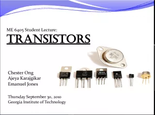
Circuit Analysis of Bipolar Junction Transistors


This article discusses the analysis of circuits using bipolar junction transistors (BJTs), including large signal DC analysis, small signal equivalent, amplifiers, operating points, and signal analysis. Our approach involves dividing the circuit into models for large signal DC analysis of BJT circuits and bias circuits for BJT amplifiers, as well as using small signal models to analyze circuits for signals being amplified.
- Uploaded on | 0 Views
-
 marisazina
About Circuit Analysis of Bipolar Junction Transistors
PowerPoint presentation about 'Circuit Analysis of Bipolar Junction Transistors'. This presentation describes the topic on This article discusses the analysis of circuits using bipolar junction transistors (BJTs), including large signal DC analysis, small signal equivalent, amplifiers, operating points, and signal analysis. Our approach involves dividing the circuit into models for large signal DC analysis of BJT circuits and bias circuits for BJT amplifiers, as well as using small signal models to analyze circuits for signals being amplified.. The key topics included in this slideshow are Bipolar Junction Transistor, Circuit Analysis, Amplifiers, DC Analysis, Small Signal Models,. Download this presentation absolutely free.
Presentation Transcript
1. Bipolar Junction Transistor Circuit Analysis Bipolar Junction Transistor Circuit Analysis EE314
2. Chapter 13: Bipolar Junction Transistors 1. Large signal DC analysis 2. Small signal equivalent 3. Amplifiers BJT Transistor Circuit Analysis
3. Circuit with BJTs Our approach: Operating point - dc operating point Analysis of the signals - the signals to be amplified Circuit is divided into: model for large-signal dc analysis of BJT circuit bias circuits for BJT amplifier small-signal models used to analyze circuits for signals being amplified Remember !
4. Large-Signal dc Analysis: Active-Region Model Important: a current-controlled current source models the dependence of the collector current on the base current The constrains for I B and V CE must be satisfy to keep BJT in the active-mode V BE forward bias V CB reverse bias ? ?
5. Large-Signal dc Analysis: Saturation-Region Model V BE forward bias V CB forward bias ? ?
6. Large-Signal dc Analysis: Cutoff-Region Model V CB reverse bias V BE reverse bias ? ? If small forward-bias voltage of up to about 0.5 V are applied, the currents are often negligible and we use the cutoff-region model.
7. Large-Signal dc Analysis: characteristics of an npn BJT
8. Large-Signal dc Analysis Procedure: (1) select the operation mode of the BJT (2) use selected model for the device to solve the circuit and determine I C , I B , V BE , and V CE (3) check to see if the solution satisfies the constrains for the region, if so the analysis is done (4) if not, assume operation in a different region and repeat until a valid solution is found This procedure is very important in the analysis and design of the bias circuit for BJT amplifier. The objective of the bias circuit is to place the operating point in the active region. Bias point it is important to select I C , I B , V BE , and V CE independent of the and operation temperature. Example 13.4, 13.5, 13.6
9. Large-Signal dc Analysis: Bias Circuit From Example 13.6 Remember: that the Q point should be independent of the stability issue) V BB & V CC provide this stability, however this impractical solution Other approach is necessary to solve this problem-resistor network V BB acts as a short circuit for ac signals
10. Large-Signal dc Analysis: Four-Resistor Bias Circuit 1 2 3 4 Thevenin equivalent Equivalent circuit for active-region model Solution of the bias problem: Input Output
11. Small-Signal Equivalent Circuit Thevenin equivalent Small signal equivalent circuit for BJT: and
12. Common Emitter Amplifier Find voltage gain: First perform DC analysis to find small-signal equivalent parameters at the operating point. Find input impedance:
13. Common Emitter Amplifier Find power gain: Find current gain Find output impedance:
14. Problem 13.13: Suppose that a certain npn transistor has V BE = 0.7V for I E =10mA. Compute V BE for I E = 1mA. Repeat for I E = 1A. Assume that V T = 26mV.
15. Problem 13.14: Consider the circuit shown in Figure P13.14. Transistors Q 1 and Q 2 are identical, both having I ES = 10 -14 A and = 100 . Calculate V BE and I C2 . Assume that V T = 26mV for both transistors. Hint: Both transistors are operating in the active region. Because the transistors are identical and have identical values of V BE , their collector currents are equal.
16. Problem 13.50: The transistors shown in Figure P13.50 operate in active region and have = 100, V BE =0.7V . Determine I C and V CE for each transistor. I 1 I E2 V BE
17. I I 1 I E Problem 13.52: Analyze the circuit of Figure P13.52 to determine I C and V CE . I B I C
18. Problem 13.45: Analyze the circuits shown in Figure P13.45 to determine I and V. For all transistors, assume that = 100 and |V BE | = 0.7V in both the active and saturation regions. Repeat for = 300 .
19. Problem 13.45: Contd.
20. I 1 Problem 13.67: Consider the emitter-follower amplifier of Figure P13.67 . Draw the dc circuit and find I CQ . Next, determine the value of r . Then, calculate midband values for A v , A voc , Z in , A i , G and Z 0 .
21. npn BJTs Practical Aspects
24. http://www.4p8.com/eric.brasse ur/vtranen.html
