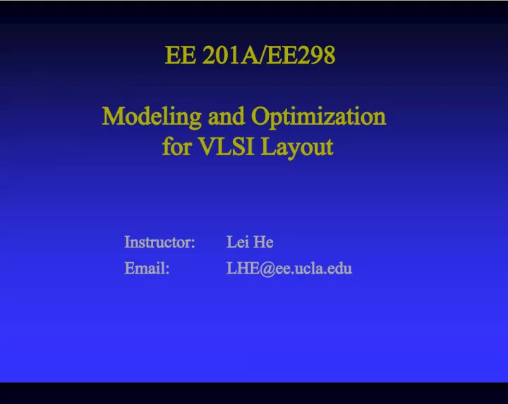
EE 201A/EE298 Modeling and Optimization for VLSI Layout

This course, taught by instructor Lei He (email: LHE@ee.ucla.edu), covers the logistics and overview of modeling and optimization for V
- Uploaded on | 1 Views
-
 scarletthughes
About EE 201A/EE298 Modeling and Optimization for VLSI Layout
PowerPoint presentation about 'EE 201A/EE298 Modeling and Optimization for VLSI Layout'. This presentation describes the topic on This course, taught by instructor Lei He (email: LHE@ee.ucla.edu), covers the logistics and overview of modeling and optimization for V. The key topics included in this slideshow are . Download this presentation absolutely free.
Presentation Transcript
Slide1EE 201A/EE298Modeling and Optimization for VLSI Layout Instructor: Lei He Email: LHE@ee.ucla.edu
Slide2Outlinen Course logistics n Course logistics n Overview n Overview What are covered in the course What are covered in the course What are interesting trends for physical design What are interesting trends for physical design
Slide3Instructor Infon Email: LHE@ee.ucla.edu n Email: LHE@ee.ucla.edu n Phone: 310-206-2037 n Phone: 310-206-2037 n Office: Engineering IV 68-117 n Office: Engineering IV 68-117 n Office hours: Tu/Th 2-3pm or by appointment n Office hours: Tu/Th 2-3pm or by appointment n The best way to reach me: n The best way to reach me: Email with EE201 in subject line Email with EE201 in subject line
Slide4About this Coursen One of selective course for EE’s ECS Major Field Students n One of selective course for EE’s ECS Major Field Students Question in M.S. comprehensive exam / PhD prelims Question in M.S. comprehensive exam / PhD prelims Offered every other spring Offered every other spring Will be under another course number (EE205B) Will be under another course number (EE205B) n Related courses n Related courses Mani’s EE202A Embedded Computing Systems (Fall) Mani’s EE202A Embedded Computing Systems (Fall) Ingrid’s EE201A on Advanced VLSI (Spring) Ingrid’s EE201A on Advanced VLSI (Spring) Bill M-S’s EE204A on Compilers (Winter) Bill M-S’s EE204A on Compilers (Winter) My EE205A Fundamental to CAD (Winter) My EE205A Fundamental to CAD (Winter) Mani’s EE206A Wireless Systems (Spring) Mani’s EE206A Wireless Systems (Spring) My EE205B (every other Spring) My EE205B (every other Spring)
Slide5Course Prerequisitesn Official prerequisite n Official prerequisite EE116B VLSI System Design EE116B VLSI System Design But mainly self-contained But mainly self-contained n Knowledge to help you appreciate more n Knowledge to help you appreciate more CS180 Introduction to algorithms CS180 Introduction to algorithms
Slide6EE205A and EE205Bn EE205A Fundamental to CAD of embedded systems n EE205A Fundamental to CAD of embedded systems System level performance/power/thermal modeling and optimization System level performance/power/thermal modeling and optimization Synthesis – scheduling and allocation, logic optimization and technology mapping Synthesis – scheduling and allocation, logic optimization and technology mapping FPGA circuits and architectures and placement and routing for FPGA FPGA circuits and architectures and placement and routing for FPGA n EE205B Modeling and Optimization for VLSI layout n EE205B Modeling and Optimization for VLSI layout Advanced algorithms for physical design Advanced algorithms for physical design Fundamentals of combinatorial algorithm Fundamentals of combinatorial algorithm Detailed performance, signal integrity, power and thermal models Detailed performance, signal integrity, power and thermal models Incorporating physical design into system design Incorporating physical design into system design
Slide7System SpecificationFunctional Design Logic Design Circuit Design X=(AB*CD)+(A+D)+(A(B+C)) Y=(A(B+C))+AC+D+A(BC+D)) VLSI Design Cycle
Slide8Physical DesignFabrication Packaging VLSI Design Cycle (cont.)
Slide9PartitionFloorplanning Placement Simplified Physical Design Cycle Routing Extraction and Verification Front-end Front-end physical design physical design Back-end Back-end physical design physical design
Slide10Course Outline and Schedulen Front-end physical design (4.5 weeks) n Front-end physical design (4.5 weeks) Partitioning, floorplanning and placement Partitioning, floorplanning and placement Power and thermal modeling Power and thermal modeling Algorithms: divided and conquer, simulated annealing, genetic algorithm Algorithms: divided and conquer, simulated annealing, genetic algorithm Project proposal due by end of fifth week Project proposal due by end of fifth week n Back-end physical design (4.5 weeks) n Back-end physical design (4.5 weeks) Interconnect extraction and modeling Interconnect extraction and modeling Interconnect synthesis Interconnect synthesis Noise modeling and avoidance Noise modeling and avoidance Clock and power supply design ** Clock and power supply design ** Algorithms: dynamic programming, linear programming Algorithms: dynamic programming, linear programming Project report due the last day of the quarter Project report due the last day of the quarter
Slide11 ACM IEEE Design Automation Conference (DAC) http://www.dac.com (San Diego, Young student program) International Conference on Computer Aided Design(ICCAD) Design, Automation and Test in Europe (DATE) Asia and South Pacific Design Automation Conference (ASP- DAC) International symposium on physical design (ISPD) International symposium on low power electronics and design International symposium on field programmable gate array IEEE International Symposium on Circuits and Systems (ISCAS) Related VLSI CAD Conferences
Slide12 IEEE Transactions on CAD of Circuits and systems (TCAD) ACM Trans. on Design Automation of Electronic Systems (TODAES) IEEE Transactions on Circuits and Systems (TCAS) IEEE Trans. on VLSI Systems (TVLSI) IEEE Trans. on Computer Integration Algorithmica SIAM journal of Discrete and Applied Mathematics Related VLSI CAD Journals
Slide13 Synposys, Cadence, Magma, Mentor Graphics, … Over hundreds companies have booths at DAC Two of them are among the ten biggest software companies in the world But they are smaller than the biggest spin-off of EDA EDA is regarded as A-graded bonds for Venture Capitalists One of few IT segments still recruits heavily and offers salary higher than Intel/IBM EDA system is regarded as one of the most complicated software systems mankind ever built Money Talk for VLSI CAD
Slide14References for this Course Selected papers from TCAD, TODAES, and major CAD conferences such as DAC, ICCAD and ISPD Selected papers from TCAD, TODAES, and major CAD conferences such as DAC, ICCAD and ISPD Naveed A. Sherwani, "Algorithms for VLSI Physical Design Automation", 3rd Edition, 1998. Naveed A. Sherwani, "Algorithms for VLSI Physical Design Automation", 3rd Edition, 1998. H. Cormen, et al “Introduction to Algorithms” MIT Electrical Engineering and Computer Science Series 1990. H. Cormen, et al “Introduction to Algorithms” MIT Electrical Engineering and Computer Science Series 1990. H. Bakoglu, Circuits, Interconnects, and Packaging for VLSI , Addison Wesley H. Bakoglu, Circuits, Interconnects, and Packaging for VLSI , Addison Wesley Cong et al., Performance Optimization of VLSI Interconnect Layout, Integration, the VLSI Journal 21 (1996) 1--94. Cong et al., Performance Optimization of VLSI Interconnect Layout, Integration, the VLSI Journal 21 (1996) 1--94.
Slide15Grading Policyn Homework 15% n Homework 15% n Midterm (7 th week) 20% n Midterm (7 th week) 20% n Course presentation 15% n Course presentation 15% n Term project 50% n Term project 50% n A score > 85 and programming project n A score > 85 and programming project
Slide16Course Presentation (15%)n 2~3 student a team n 2~3 student a team n Survey an area (topics and resources specified by me on a continual basis) n Survey an area (topics and resources specified by me on a continual basis) n Prepare slides and do a 30-35 minute presentation in the class n Prepare slides and do a 30-35 minute presentation in the class slides prepared jointly slides prepared jointly either all students share the presentation or I will select the speaker randomly at the presentation time either all students share the presentation or I will select the speaker randomly at the presentation time n Prepare a web site that should contain a report based on your survey, a bibliography, and links to resources and of course your slides n Prepare a web site that should contain a report based on your survey, a bibliography, and links to resources and of course your slides
Slide17Term Project (50%) One of the following two: One of the following two: One-person survey and critic of selected topic (at most 35%) One-person survey and critic of selected topic (at most 35%) Individual programming project for a team of 2 to 3 persons Individual programming project for a team of 2 to 3 persons Coupled system design and physical design Coupled system design and physical design Floorplanning with thermal constraints Floorplanning with thermal constraints 3D modeling and physical design 3D modeling and physical design Or any topic agreed by instructor Or any topic agreed by instructor n Up to 30 minute presentation during the finals week, like a conference talk n Up to 30 minute presentation during the finals week, like a conference talk n Up to 12 page report in the style of a technical conference paper n Up to 12 page report in the style of a technical conference paper ACM style http://www.acm.org/sigs/pubs/proceed/template.htm ACM style http://www.acm.org/sigs/pubs/proceed/template.htm
Slide18Who should take this coursen It is another course n It is another course Discuss wide scope of knowledge Discuss wide scope of knowledge But research (presentation + project) on your own focus But research (presentation + project) on your own focus n For students who are motivated to n For students who are motivated to Learn SI, power/thermal for advanced designs Learn SI, power/thermal for advanced designs Learn algorithm basics without taking CS280 Learn algorithm basics without taking CS280 Understand CAD better Understand CAD better Become a CAD professional Become a CAD professional
Slide19 More than 10 million transistor Performance driven designs Time-to-Market Design cycle High performance, high cost …... Complexities of Physical Design
Slide20Moore’s Law and NTRSn Moore’s Law n Moore’s Law The min. transistor feature size decreases by 0.7X every three years (Electronics Magazine, Vol. 38, April 1965) The min. transistor feature size decreases by 0.7X every three years (Electronics Magazine, Vol. 38, April 1965) True in the past 30 years, and expected to hold for another 10- 15 years True in the past 30 years, and expected to hold for another 10- 15 years n National Technology Roadmap for Semiconductors (NTRS’97) n National Technology Roadmap for Semiconductors (NTRS’97)
Slide21Productivity Gapx x x x x x x 21%/Yr. Productivity growth rate x 58%/Yr. Complexity growth rate 1 10 100 1,000 10,000 100,000 1,000,000 10,000,000 1998 10 100 1,000 10,000 100,000 1,000,000 10,000,000 100,000,000 Logic Transistors/Chip (K) Transistor/Staff-Month Chip Capacity and Designer Productivity 2003 Source: NTRS’97
Slide22Design Challenges in Nanometer Technologiesn Interconnect-limited designs n Interconnect-limited designs Interconnect performance limitation Interconnect performance limitation Interconnect modeling complexity Interconnect modeling complexity Interconnect reliability Interconnect reliability Impact of new interconnect materials Impact of new interconnect materials n Small feature size n Small feature size Process variations Process variations Leakage (~50% of total power) Leakage (~50% of total power) n High degree of on-chip integration n High degree of on-chip integration Complexity and productivity Complexity and productivity Limitation of current design abstraction and hierarchy Limitation of current design abstraction and hierarchy System on a chip and system in package or 3D technology System on a chip and system in package or 3D technology Power/thermal barrier Power/thermal barrier
Slide23Complexity ofVLSI circuits Full custom Performance Size Cost Market time Standard Cell Gate Array FPGA Different design styles Cost ,Flexibility,Performance Design Styles
Slide24Full Custom Design StylePad Metal Via Metal 2 I/O Data Path ROM/RAM PLA A/D Converter Random logic
Slide25Standard Cell Design StyleVDD Metal 1 Cell Metal 2 Feedthrough GND D C C B A C C D C D B C C C B Cell A Cell C Cell B Cell D Feedthrough cell
Slide26Gate Array Design Style (or Structured ASIC)A B C A B C VDD Metal1 Metal2
Slide27 Programmable logic Programmable interconnects Programmable inputs/outputs Field-Programmable Gate-Arrays (FPGAs)
Slide28FPGA Design Style
Slide29Comparisons of Design Styles* uneven height cells are also used style
Slide30AreaPerformance Fabrication layers style full-custom standard cell gate array FPGA compact high compact to moderate moderate large high to moderate moderate low ALL ALL routing layers none Comparisons of Design Styles
Slide31Printed Circuit BoardPCB Multi-Chip Module MCM Wafer Scale Integration WSI or 3D Packaging Area Performance, cost The increasing complexity and density of the semiconductor devices are driving the development of more advanced VLSI packaging and interconnection approaches. Packaging Styles
Slide32Printed Circuit Board Model Large number of layers (150a pitch) Larger area Low performance Low cost Package Plated through holes IC ( a ) ( b )
Slide33MCM Model Up to 36 layers ( 75a pitch) Moderate to small area Moderate to high performance High cost Heat dissipation problems IC ( a ) ( b )
Slide34Wafer Scale Integration Small number of layers (VLSI technology- 6a pitch) Smallest area Significant yield problems Very high performance Significant heat dissipation problems
Slide35Comparisons of Packaging Styles Merit = propagation speed (inches/psec.) * interconnection density (inches/sq. in). Interconnect resistance was not considered
Slide36Increasingly on the Same Chip or in theSame Package (SoC and SiP) n SC3001 DIRAC chip (Sirius Communications) n SC3001 DIRAC chip (Sirius Communications)
Slide37History of VLSI Layout ToolsOne of the new trends: SoC and SiP for 3D technology
Slide38Summary Physical design is the most complicated step in the VLSI design cycle Physical design is the most complicated step in the VLSI design cycle Physical design is further divided into clustering, partitioning, floorplanning, placement, global and detailed routing. Extraction and verification is an important aspect. Physical design is further divided into clustering, partitioning, floorplanning, placement, global and detailed routing. Extraction and verification is an important aspect. There are four major design styles -- full custom, standard cell, gate array (structured ASIC), and FPGAs. There are four major design styles -- full custom, standard cell, gate array (structured ASIC), and FPGAs. There are three alternatives for packaging of chips -- PCB, MCM and WSI. But increasingly, we design for SoC and SiP and will use 3D technology There are three alternatives for packaging of chips -- PCB, MCM and WSI. But increasingly, we design for SoC and SiP and will use 3D technology Automation reduces cost, increases chip density, reduces time-to-market, and improves performance. Automation reduces cost, increases chip density, reduces time-to-market, and improves performance. CAD tools currently lag behind fabrication technology, which is hindering the progress of IC technology CAD tools currently lag behind fabrication technology, which is hindering the progress of IC technology
Slide39Homework (due April 14th ) Read ITRS roadmap executive summary and write one page summary and critic on one aspect related to your research or field Read ITRS roadmap executive summary and write one page summary and critic on one aspect related to your research or field http://public.itrs.net/Files/2001ITRS/Home.htm http://public.itrs.net/Files/2001ITRS/Home.htm Search literature or web related to SoC, SiP and 3D technology, summarize five papers on a coherent topic (e.g., technology, design, or CAD) and speculate potential need of CAD research Search literature or web related to SoC, SiP and 3D technology, summarize five papers on a coherent topic (e.g., technology, design, or CAD) and speculate potential need of CAD research Following style of conference paper Following style of conference paper With course project proposal in mind With course project proposal in mind Submit homework in PDF via email Submit homework in PDF via email Check out course website for notes of future lectures Check out course website for notes of future lectures http://eda.ee.ucla.edu/EE201A-04Spring http://eda.ee.ucla.edu/EE201A-04Spring
