Transistor Fundamentals: Understanding the Basics of Transistors

The ME 6405 Student Lecture at the Georgia Institute of Technology on Thursday, September 30, 2010, focused on Transistor Fundamentals. The lecture
- Uploaded on | 6 Views
-
 deanbrewer
About Transistor Fundamentals: Understanding the Basics of Transistors
PowerPoint presentation about 'Transistor Fundamentals: Understanding the Basics of Transistors'. This presentation describes the topic on The ME 6405 Student Lecture at the Georgia Institute of Technology on Thursday, September 30, 2010, focused on Transistor Fundamentals. The lecture. The key topics included in this slideshow are . Download this presentation absolutely free.
Presentation Transcript
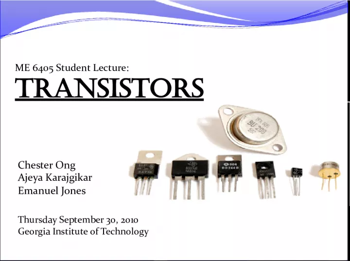
Slide1ME 6405 Student Lecture:Transistors Chester Ong Ajeya Karajgikar Emanuel Jones Thursday September 30, 2010 Georgia Institute of Technology
Slide2Transistor FundamentalsChester Ong Power Transistors Ajeya Karajgikar Field Effect Transistors Emanuel Jones 1 1 3 3 4 4 Applications of Transistor (covered by each speaker in respective topic) 5 5 Bipolar Junction Transistors Ajeya Karajgikar 2 2 Presentation Outline
Slide3TransistorsFirst Transistor Model, 1947 FET Transistor BJT Transistor Transistors of various type & size Used in all modern electronics BJT (PNP) Electrical Diagram Representation
Slide41. What is a Transistor?• Basic Purpose of a Transistor • Recognize Transistor Role in Modern Electronics • Understand Reason(s) for its Invention • Comparison to its “predecessor,” the Vacuum Tube 2. How are transistors made? • “Doping” Manufacturing Process • Effect of Doping on Semiconductors • Creation of a P-N Junction via Doping 3. How do transistors work? • Depletion Region of a P-N Junction • How to Control Current through a Depletion Region • How a P-N Junction can act as an Electrical Switch • Combination of P-N Junctions -> Transistors Understanding Transistors (conceptually)
Slide5Basic Purpose [1] To amplify signals [2] To electronically switch (no moving parts) a signal on or off (high/low) Role in Modern Electronics • Basic building blocks for all modern electronics • Microprocessors, Microcontrollers, Computers, Digital watches, Digital Logic Circuits, Cell Phones…. What is a Transistor? Microprocessor PC & Cell Phones Motor Controllers Headphones
Slide6Early 20 th century, vacuum tube was used for signal amplifier & switch. U se of vacuum tube* resulted in extremely large, fragile, energy inefficient, and expensive electronics. Evolution of electronics required device that was small, light weight, robust, reliable, cheap to manufacture, energy efficient: *Vacuum tube advantages: operation at higher voltages (10K region vs. 1K region of transistors); high power, high frequency operation (over-the-air TV broadcasting) better suited for vacuum tubes; and silicon transistors more vulnerable to electromagnetic pulses than vacuum tubes Reason for Transistor’s Invention: Vacuum Tube Radios ENIAC : 17, 468 vacuum tubes
Slide7Invention In 1947, John Bardeen, Walter Brattain, and William Schockly, researchers at Bell Lab, invented Transistor. They found Transistor Effect: “when electrical contacts were applied to a crystal of germanium, the output power was larger than the input.” Awarded the Nobel Prize in physics (1956) Transistor is a semiconductor device commonly used to amplify or switch electronic signals. John Bardeen, Walter Brattain, and William Schockly First model of Transistor, 1947 …and the TRANSISTOR was born!
Slide8more than 2.9 billion transistors ispacked into an area of fingernail 1941, Vacuum Tube 1948, the first (Germanium) TR 1954, Silicon TR 1958, Integrated Circuit Sep 2009, 22nm silicon wafer John Bardeen, Walter Brattain, and William Schockly At TI Lab, Ease of processing, lower cost, greater power handling, more stable temperature characteristics Intel CEO Paul Otellini, Sep 23 2009 Individual electronic components were soldered on to printed circuit boards. IC placed all components in one chip. Historical Development
Slide9Transistor are categorized by • Semiconductor material: germanium, silicon, gallium arsenide, etc. • Structure: BJT, FET, IGFET (MOSFET), IGBT • Polarity: NPN, PNP (BJTs); N-channel, P-channel (FETs) • Maximum power rating: low, medium, high • Maximum operating frequency: low, medium, high • Application: switch, audio, high voltage, etc. • Physical packaging: through hole, surface mount, ball grid array, etc. • Amplification factor Various Types of Transistor: http://en.wikipedia.org/wiki/Category:Transistor_types Various Types of Transistors • Bipolar Junction Transistor (BJT) • Field Effect Transistors (FET) • Power Transistors Transistor Categories and Types
Slide101. What is a Transistor?• Basic Purpose of a Transistor • Recognize Transistor Role in Modern Electronics • Understand Reason(s) for its Invention • Comparison to its “predecessor,” the Vacuum Tube 2. How are transistors made? • “Doping” Manufacturing Process • Effect of Doping on Semiconductors • Creation of a P-N Junction via Doping 3. How do transistors work? • Depletion Region of a P-N Junction • How to Control Current through a Depletion Region • How a P-N Junction can act as an Electrical Switch • Combination of P-N Junctions -> Transistors Understanding Transistors (conceptually)
Slide11Doping Manufacturing ProcessDoping: “ Process of introducing impure elements (dopants) into semiconductor wafers to form regions of differing electrical conductivity.” Two Main Manufacturing Processes: [1] High-temperature furnace diffuse a solid layer of “dopant” onto wafer surface. [2] Ion implanter: gaseous dopants are ionized (stripped of electrons); accelerated using an electric field; and deposited in a silicon wafer. Ion Implanter Wafer Refinement High-Temp Furnace “Pure” Wafers “Doped” Wafers
Slide12Effect of Doping on Semi-Conductors(1/3) General Characteristics of Semiconductors : • Possesses an electrical conductivity somewhere between insulators & conductors • Typical material composition is either silicon or germanium • Semiconductors are more “insulators” than “conductors,” since semiconductors possess few free electrons (as opposed to conductors, which have many free electrons) Doping impurities into a “pure”semiconductor will increase conductivity . Doping results in an “ N-Type ” or “ P-Type ” semiconductor.
Slide13Effect of Doping on Semi-Conductors(2/3) P-Type Semiconductors : P ositively charged Semiconductor Dopant Material: Boron, Aluminum, Gallium Effect of Dopant: • “takes away” weakly-bound outer orbit electrons from semiconductor atom. • Semiconductor now has “missing” electron or “ hole ” in its lattice structure. • Overall material is now positively charged , because material has fewer electrons but still wants to accept electrons to fill holes in its lattice structure
Slide14Effect of Doping on Semi-Conductors(3/3) N-Type Semiconductors : N egatively charged Semiconductor Dopant Material: Phosphorous, Arsenic, Antimony (Sb) Effect of Dopant: • “ adds” electrons to semiconductor atom • Semiconductor is now negatively charged , because of electron abundance • Overall material (semiconductor + dopant) wants to donate “extra” electrons to make lattice structure at its lowest energy state
Slide15Creation of P-N Junction via Doping Remember: Doping introduces impurities into semiconductor material Remember: Dopant is added to same piece of semiconductor material Resulting Material : Single, solid material called “ P-N Junction ” Example: Boron (P-Type) to side A and Antimony (N-Type) to side B Positively-charged P-type Side Lattice structure wants electrons to fill “holes” What happens at the point of contact or “junction? Lattice structure has too many electrons Negatively-charged N-type Side
Slide161. What is a Transistor?• Basic Purpose of a Transistor • Recognize Transistor Role in Modern Electronics • Understand Reason(s) for its Invention • Comparison to its “predecessor,” the Vacuum Tube 2. How are transistors made? • “Doping” Manufacturing Process • Effect of Doping on Semiconductors • Creation of a P-N Junction via Doping 3. How do transistors work? • Depletion Region of a P-N Junction • How to Control Current through a Depletion Region • How a P-N Junction can act as an Electrical Switch • Combination of P-N Junctions -> Transistors Understanding Transistors (conceptually)
Slide17Depletion Region of P-N Junction At equilibrium with no external voltage , a thin and constant-thickness “depletion region” forms between P-type and N-type semiconductors . In depletion region, free electrons from N-type will “fill” the electron holes in the P-type until equilibrium. Negative and positive ions are subsequently created in depletion region. Ions exhibit a (Coulomb) force which inhibits further electron flow (i.e. current) across the P-N Junction unless a forward bias external voltage is applied.
Slide18Current through a Depletion Region Remember: • Depletion region is created at equilibrium between P & N-type junction. • Positive & negative ions are created in depletion region. • Ions have a Coulomb force which impedes motion of electrons – essentially insulator property. Applying External Voltage… • …of Forward Biasing polarity facilitates motion of free electrons -> Coulomb force is overcome, electrons flow from N to P • …of Reverse Biasing polarity impedes motion of free electrons -> No current flow because of Coulomb force in depletion region
Slide19Electrical Switching on P-N Junction Applying External Voltage… • …of Forward Biasing polarity facilitates motion of free electrons • …of Reverse Biasing polarity impedes motion of free electrons Reverse Biasing Forward Biasing • Circuit is “Off” • Current not Flowing • Circuit is “On” • Current is Flowing
Slide20Finally – combining all concepts Semiconductor -> Doping -> P-N Junction -> Depletion Region -> Ions & Coulomb Force -> External Voltage -> Current on/off One P-N Junction can control current flow via an external voltage Two P-N junctions ( bipolar junction transistor, BJT) can control current flow and amplify the current flow. Also, if a resistor is attached to the output, the resulting voltage output is much greater than the applied voltage, due to amplified current and I*R=V.
Slide21Transistor FundamentalsChester Ong Power Transistors Ajeya Karajgikar Field Effect Transistors Emanuel Jones 1 1 3 3 4 4 Applications of Transistor (covered by each speaker in respective topic) 5 5 Bipolar Junction Transistors Ajeya Karajgikar 2 2 Presentation Outline
Slide22BJT introduction BJT = B ipolar J unction T ransistor 3 Terminals Base (B) Collector (C) Emitter (E)
Slide23NPNPNP NPN: BE forward biased BC reverse biased PNP: BE reverse biased BC forward biased BJT schematic
Slide24BJT formulaeNPN Current control β is the amplification factor and ranges from 20 to 200 It is dependent on temperature and voltage
Slide25BJT formulaeNPN Emitter is more heavily doped than the collector. Therefore, V C > V B > V E for NPN transistor
Slide26BJT formulaeNPN α is the fraction of electrons that diffuse across the narrow base region 1 – α is the fraction of electrons that recombine with holes in the base region to create base current
Slide27Common Emitter Transistor Circuit Emitter is grounded and input voltage is applied to Base Base-Emitter starts to conduct when V BE is about 0.6V, i C flows with i C = β.i B As i B further increases, V BE slowly increases to 0.7V, i C rises exponentially As i C rises, voltage drop across R C increases and V CE drops toward ground (transistor in saturation, no more linear relation between i C and i B ) 27
Slide28Common Emitter Characteristics28 No current flows Collector current controlled by the collector circuit ( Switch behavior ) In full saturation V CE =0.2V Collector current I C proportional to Base current I B
Slide29BJT operating regionsOperating Region Parameters Mode Cut Off V BE < V cut-in V CE > V supply I B = I C = 0 Switch OFF Linear V BE = V cut-in V sat < V CE < V supply I C = β * I B Amplification Saturated V BE = V cut-in , V CE < V sat I B > I C,max , I C,max > 0 Switch ON
Slide30VSupply V in R B R C BJT as an amplifier Question: What is the minimum V in that makes the transistor act as an amplifier? Given: • R B = 10 k Ω • R C = 1 k Ω • β = 100 • V Supply = 10 V • V cut-in = 0.7 V • V sat = 0.2 V i B = i C / β = 0.0098/100 = 0.098 mA V in – i B . R B – V BE = 0 V supply – i C . R C – V CE = 0 i C = ( V supply – V CE ) / R C Set V CE = V sat = 0.2V i C = (10 – 0.2) / 1000 = 9.8 mA i C = β . i B V in = i B . R B + V BE Set V BE = V cut-in = 0.7V V in = (0.098) .(10 -3 ).(10000 )+ 0.7V V in = 1.68 V or greater. I II II I
Slide31BJT as a switch• From exercise 3 • Turns on/off coils digitally
Slide32Power Transistors Concerned with delivering high power Used in high voltage and high current application In general Fabrication process different in order to: Dissipate more heat Avoid breakdown Different types: Power BJTs, power MOSFETS, etc.
Slide33Transistor FundamentalsChester Ong Power Transistors Ajeya Karajgikar Field Effect Transistors Emanuel Jones 1 1 3 3 4 4 Applications of Transistor (covered by each speaker in respective topic) 5 5 Bipolar Junction Transistors Ajeya Karajgikar 2 2 Presentation Outline
Slide34Presented by: Emanuel Jones
Slide35• Semiconductor device that depends on electric field to control the current • Performs same functions as a BJT; amplifier, switch, etc. • Relies on PNP or NPN junctions to allow current flow • However, mechanism that controls current is different from the BJT • Remember the BJT is bipolar . The FET is sometimes called a unipolar transistor • One type of charge carrier
Slide36• FETs have three main parts • Drain • Source • Gate • The body has contacts at the ends: the drain and source • Gate surrounds the body and can induce a channel to because of an electric field FET BJT Input voltage controls output current Input current controls output current Gate Base Controls flow of current Drain Collector Current goes out here Source Emitter Current comes in here
Slide37Simplified NotationNo current flow “Short” allows current flow No Voltage to Gate Voltage to Gate MOSFET shown here Source Source Drain Drain n n
Slide38Types of Field-Effect TransistorsMOSFET IGBT Type Function J unction F ield- E ffect T ransistor (JFET) Uses reversed biased p-n junction to separate gate from body M etal- O xide- S emiconductor FET (MOSFET) Uses insulator (usu. SiO 2 ) between gate and body I nsulated G ate B ipolar T ransistor (IGBT) Similar to MOSFET, but different main channel O rganic F ield- E ffect T ransistor (OFET) Uses organic semiconductor in its channel N anoparticle O rganic M emory FET (NOMFET) Combines the organic transistor and gold nanoparticles “ DNAFET ” Uses a gate made of single-strand DNA molecules
Slide39JFET A single channel of single doped SC material with terminals at end Gate surrounds channel with doping that is opposite of the channel, making the PNP or NPN type Uses reversed biased p-n junction to separate gate from body Flow of current is similar to water flow through a garden hose Pinch the hose (decrease current channel width) to decrease flow Open the hose (increase channel width) to increase flow Also, the pressure differential from the front and back of the hose (synonymous with the voltage from drain to source) effects the flow n-channel JFET p-channel JFET
Slide40JFET analysisI–V characteristics and output plot of a JFET n-channel transistor.
Slide41JFET analysisI DS : Drain current in saturation region V GS : Voltage at the gate V th : Threshold voltage V DS : Voltage from drain to source V P : Pinch-off voltage [1] [1] - This "pinch-off voltage" varies considerably, even among devices of the same type. For example, V GS(off) for the Temic J201 device varies from -0.8V to -4V. Typical values vary from -0.3V to -10V.
Slide42MOSFET Similar to JFET – remember… A single channel of single doped SC material with terminals at end Gate surrounds channel with doping that is opposite of the channel, making the PNP or NPN type BUT, the MOSFET uses an insulator to separate gate from body, while JFET uses a reverse-bias p-n junction p-channel n-channel MOSFET enhanced mode MOSFET depleted mode
Slide43MOSFETFETs vary voltage to control current. This illustrates how that works MOSFET drain current vs. drain-to-source voltage for several values of V GS − V th ; the boundary between linear ( Ohmic ) and saturation ( active ) modes is indicated by the upward curving parabola.
Slide44MOSFETTriode Mode/Linear Region V GS > V th and V DS < ( V GS - V th ) V GS : Voltage at the gate V th : Threshold voltage V DS : Voltage from drain to source μ n : charge-carrier effective mobility W : gate width L : gate length C ox : gate oxide capacitance per unit area λ : channel-length modulation parameter Saturation/Active Mode V GS > V th and V DS > ( V GS - V th )
Slide45Characteristics and Applications of FETsJFETs • Simplest type of FET – easy to make • High input resistance • Low Capacitance • High input impedance • Slower speed in switching • Uses? – Displacement sensor – High input impedance amplifier – Low-noise amplifier – Analog switch – Voltage controlled resistor
Slide46Characteristics and Applications of FETsMOSFETs • Oxide layer prevents DC current from flowing through gate • Reduces power consumption • High input impedance • Rapid switching • More noise than JFET • Uses? • Again, switches and amplifiers in general • The MOSFET is used in digital CMOS logic, which uses p- and n- channel MOSFETs as building blocks • To aid in negating effects that cause discharge of batteries Use of MOSFET in battery protection circuit
Slide47Transistor Fundamentals Chester Ong Power Transistors Ajeya Karajgikar Field Effect Transistor Emanuel Jones 1 1 3 3 4 4 Applications of Transistor (covered by each speaker in respective topic) 5 5 Bipolar Junction Transistors Ajeya Karajgikar 2 2 Presentation Summary • Use of electric field to change the output current • JFETs and MOSFETs are most common, and accomplish similar goals as BJTs • Used for switches, amplification, applications for protecting electronics • Definition and Applications • Introduction & Formulae • Explain function and characteristics of common emitter transistor • Describe BJT operating regions • Applications of BJTs • Qualitative explanation of the what & how behind transistors • General application and history of transistors • “Physics” behind transistors : Doping Process, Effect on Semiconductors, & Formation of P-N Junction Electrical Properties of P-N Junction & using P-N to control / amplify current
Slide48References (32) 1. http://www.utdallas.edu/research/cleanroom/TystarFurnace.htm 2. http://www.osha.gov/SLTC/semiconductors/definitions.html 3. http://www.products.cvdequipment.com/applications/diffusion/1/ 4. http://amath.colorado.edu/index.php?page=an-immersed-interface-method-for-modeling-semiconductor-devices 5. http://www.extremetech.com/article2/0,2845,1938467,00.asp 6. http://macao.communications.museum/eng/Exhibition/secondfloor/moreinfo/2_10_3_HowTransistorWorks.html 7. http://fourier.eng.hmc.edu/e84/lectures/ch4/node3.html 8. http://www.appliedmaterials.com/htmat/animated.html really good video! 9. http://hyperphysics.phy-astr.gsu.edu/hbase/solids/dope.html#c3 10. http://www.tpub.com/neets/book7/25.htm 11. http://esminfo.prenhall.com/engineering/wakerlyinfo/samples/BJT.pdf 12. http://web.engr.oregonstate.edu/~traylor/ece112/lectures/bjt_reg_of_op.pdf 13. http://www.me.gatech.edu/mechatronics_course/transistors_F09.ppt 14. http://en.wikipedia.org/wiki/Bipolar_junction_transistor 15. http://en.wikipedia.org/wiki/Common_emitter 16. http://en.wikipedia.org/wiki/Diode 17. http://www.kpsec.freeuk.com/trancirc.htm 18. http://en.wikipedia.org/wiki/Field-effect_transistor 19. http://en.wikipedia.org/wiki/JFET 20. http://en.wikipedia.org/wiki/MOSFET 21. http://www.slideshare.net/guest3b5d8a/fets 22. http://www.rhopointcomponents.com/images/jfetapps.pdf 23. http://cnx.org/content/m1030/latest/ 24. http://www.play-hookey.com/semiconductors/enhancement_mode_mosfet.html 25. http://www.youtube.com/watch?v=-aHnmHwa_6I&feature=related 26. http://www.youtube.com/watch?v=v7J_snw0Eng&feature=related 27. http://info.tuwien.ac.at/theochem/si-srtio3_interface/si-srtio3.html 28. http://hyperphysics.phy-astr.gsu.edu/hbase/solids/dope.html#c4 29. http://inventors.about.com/library/inventors/blsolar5.htm 30. http://thalia.spec.gmu.edu/~pparis/classes/notes_101/node100.html 31. http://hyperphysics.phy-astr.gsu.edu/hbase/solids/pnjun.html#c3 32. http://science.jrank.org/pages/6925/Transistor.html - also really good explanation!
Slide49Questions?Thank you!